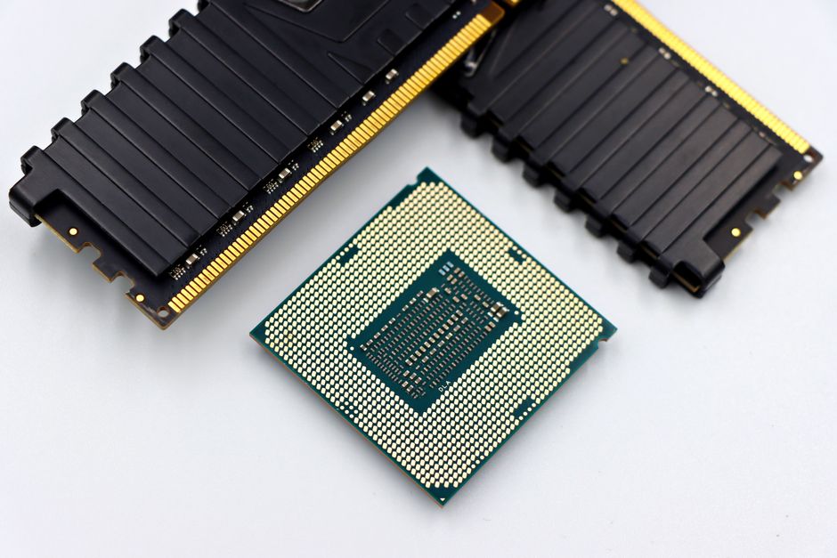
SK hynix and SanDisk have introduced a new High Bandwidth Flash (HBF) standard designed to resolve performance gaps between High Bandwidth Memory (HBM) and SSDs in AI accelerators. The standard was specifically developed for AI inference scenarios where Large Language Models (LLMs) are run. source_ref:1,11
HBF is designed to complement HBM capacity limits rather than replace them. Unlike HBM, HBF utilizes stacked NAND flash instead of DRAM to increase storage capacity. source_ref:4,3
The HBF standard supports the UCIe (Universal Chiplet Interconnect Express) specification and aims to create an ecosystem where various enterprises can develop compatible products. The technology is currently supported by Google and Tenstorrent. source_ref:7,2,10
Capacity and technical specifications
A 16-layer HBF stack can provide 512 GB of capacity in a package similar in size to HBM. Specifications allow for up to 512GB in a single configuration. source_ref:12,5
SanDisk stated that HBF can provide 8 to 16 times more capacity than HBM at similar cost levels. source_ref:13
Market competition and roadmap
Samsung is developing and mass-producing CMX solutions and manufacturing V10 and V11 NAND flash with up to 500 stacked layers to target AI server storage requirements. source_ref:9
SanDisk aims to have the first HBF samples ready in the second half of 2026, with the first AI inference hardware using HBF technology planned for sampling in early 2027. source_ref:14,15
Updates
The HBF specification has been released through the Open Compute Project (OCP), covering detailed performance requirements, electrical design rules, and software guidelines. According to SK hynix, the standard utilizes the Universal Chiplet Interconnect Express (UCIe) to simplify integration, with high-end implementations expected to provide 3 TB/s of bandwidth—surpassing the 2 TB/s bandwidth of a single HBM4 memory stack. Additionally, SanDisk claims the technology is set to adopt the 'xPU-HBF' interface.
The HBF specification has been released through the Open Compute Project (OCP) and encompasses detailed performance requirements, electrical design rules, packaging methods, and software guidelines. SK hynix claims that the standard utilizes the Universal Chiplet Interconnect Express (UCIe) to simplify heterogeneous computing integration, with a single UCIe interface potentially reaching over 400 GB/s of bandwidth. Furthermore, the most capable HBF implementation is expected to provide 3 TB/s of bandwidth, exceeding the 2 TB/s bandwidth of a single HBM4 memory stack.
The HBF specification has been released through the Open Compute Project (OCP), detailing everything from performance requirements and electrical design rules to software guidelines and packaging methods. SK hynix confirms the standard utilizes the Universal Chiplet Interconnect Express (UCIe) for easier integration, while SanDisk claims the technology will adopt a 'xPU-HBF' interface. Furthermore, the most capable HBF implementation is expected to provide 3 TB/s of bandwidth, surpassing the 2 TB/s memory bandwidth of a single HBM4 stack.
The HBF specification, released through the Open Compute Project (OCP), encompasses performance requirements, electrical design rules, packaging methods, and software guidelines. To simplify integration with heterogeneous computing platforms, SK hynix states that HBF utilizes the Universal Chiplet Interconnect Express (UCIe) standard. Additionally, SanDisk claims the standard is set to adopt the 'xPU-HBF' interface, while the most capable implementation is expected to provide 3 TB/s of bandwidth, exceeding the 2 TB/s limit of a single HBM4 memory stack.